Overclocking Linksys EA-Series Routers
Embedded electronics are ubiquitous to modern life. Many of the devices that are in the home that, at first glance, appear to be single use appliances but are actually very capable general purpose computers. Such is the case with home network devices like the router you have controlling your home network. With a some knowledge and confidence, you can take your home router to the next level.
Table of Contents
- Introduction and Background
- Overclocking Guide
- Step by Step Guide
- Clock Configuration Tables
- Links
Introduction and Background
Why should we overclock a router?
Overclocking your router has the potential to increase the performance of your home network given that the performance of your router is the bottleneck. It will usually increase throughput of your PPPoE and NAT services. I have OpenWRT flashed onto the routers that I have overclocked and they work great as Wifi repeaters, OpenVPN, etc. It’s also nice to have a powerful and cheap travel router so I can have a proper firewall and VPN behind my devices on public networks. Routers like the EA3500 can be had for the price of shipping on eBay and when overclocked perform not too far off from much newer more expensive routers.
Why can we overclock a router?
The answer boils down to economies of scale. Rather than have proprietary CPUs and systems for each type of embedded device, it’s actually cheaper and simpler to have each of these “single purpose” devices use the same underlying chipset. A common way to take advantage of economies of scale for embedded devices is to use a System on a Chip (SoC) which contains much of the needed hardware to accomplish many different tasks. The SoC is a cheap and reusable way to allow many different types of devices such as routers, phones, smart TVs, etc. to all use the same chip rather than having to spend lots of money on the engineering involved to create proprietary silicon for every different use-case. Different use-cases have different performance/power/heat requirements and as a result SoCs often support a wide range of clock speed configurations. So it happens that the SoC that is running at a low clock speed in a router, may also be the same SoC that is running in a smart TV at a higher clock speed. Also, manufacturers like to have cheaper and more expensive models of the same device to widen their customer base, and one tactic is to simply down-clock a perfectly capable device as I’ll explain more on below.
Marvell Feroceon 88F6282 SoC
The Linksys EA3500 and EA4200 / EA4500 use the Marvell Feroceon 88F6282 SoC is used in a wide variety of devices ranging from home routers to network attached storage devices. The datasheet for the Marvell chip mentions a large variety of use cases for the SoC, which you can read about in the product overview PDF.
When a manufacturer chooses to use a SoC for the brains of their device, they usually only enable the features that best fits needs of the device. In our case, the Linksys EA3500 / EA4x00 is a network router so it needs to have good networking capability, but not much else. There’s no need for any SATA ports, displays, sound, etc. so that un-needed functionality is left disconnected. In some cases it’s possible to expose that disconnected functionality, but that’s another blog post.
Pros and Cons of Overclocking
Clock speed is a trade off between performance and heat / power consumption where the higher the clock speed the more performance but also the more power consumption and heat that needs to be dissipated. In the case of this router, most home internet connections around the time this router was manufactured (~2011) were probably less than 100Mbs, and we don’t need stellar performance to support a WAN connection that is around that speed. Also when choosing device clock speed, the manufacturer needs to consider where this device is going to be placed inside the home. A home router is a set-it-and-forget-it type of device that needs to be reliable and needs to work in many different environments. A happy medium was probably chosen at 800MHz so that the device has adequate performance and doesn’t overheat when it is sitting in someone’s enclosed cabinet.
I’ll also mention that there is a business side to the clock speed choice. The EA3500 is the “lesser” model of the two Linksys devices using the Feroceon SoC. The Linksys EA3500 is clocked at 800MHz; however, the EA4x00 is clocked 400MHz higher at 1200MHz. There is no technical reason that I can articulate to describe why the EA3500 can’t also be clocked at 1200MHz. This leads me to believe that the lower clock speed was purely a business decision to justify having two models and to charge more for the “better” EA4x00. To be fair, I should also note that the EA4x00 had 128MB or ram vs. the 64MB of the EA3500, so that’s at least one technical reason to charge more but this has less of an impact to performance in my experience.
Overclocking Guide
Overclocking the Linksys EA3500 and EA4x00 (EA4200 / EA4500) are virtually the same process since the use the same SoC; however, they support different clock rates and have different PCB layouts so this guide splits off where the two devices differ.
Disclaimer
By following this guide you are assuming any risk which may result in your device being permanently damaged or destroyed. Soldering and working with electronics can be dangerous if you don’t know what you’re doing. Do not attempt this if you do not understand the risks involved.
Clock Configuration on the Marvell Feroceon 88F6282
The Marvell Feroceon SoC clock speed is programmatically configured when the device is booted. There are a series of multiplexed pins on the SoC that when pulled high or low determine the CPU clock speed, as well as the ratios of CPU to DDR speed and CPU to L2 Cache speed. These pins are referred to as “MPP” in the datasheet.
These MPPs are used for other functions on the device such as the NAND flash functionality among others. Because of this, we can derive which pins need to be pulled high or low to give us the desired CPU clock speed and DDR, L2 ratios by looking at the datasheet for the NAND flash to understand it’s pin-out.
The Marvell Feroceon has default internal configuration using 50k ohm resistors, and the manufacturer is able to override this configuration by using 4.7k ohm resistors to pull the appropriate MPP high or low. We have access to override the internal configuration as long as the manufacturer has exposed the configuration pins on the board. Unfortunately, if the manufacturer doesn’t expose these configuration pins, then we are unable to change the internal configuration. Luckily, for the Linksys EA3500 and EA4x00, the pins that we need to access are exposed.
Step By Step Guide
Prerequisites
You should flash any custom firmware first before attempting to overclock your router.
I would highly recommend OpenWrt as it is much more capable and secure than the stock firmware.
- OpenWrt
- Serial to USB adapter (or serial port)
- (This is optional but highly recommended as it will help you debug if there are any issues)
- Soldering iron
- A fine point tip works best
- Small jewelers flathead screw driver
- (for extracting the SMD resistors)
- Multimeter (Optional)
- Highly recommended to ensure continuity and proper connections
- 4.7k ohm resistor (Optional for EA3500)
- Required for EA4x00 and recommended for EA3500 in case you loose a SMD resistor
- Bench Magnifying Glass / Lots of Light (Optional)
- This will help you see the SMD resistors which are not much larger than the width of a human hair. I didn’t use a magnifying glass, but I’ve been doing this for a while and have some practice with small electronics.
Target Clock Speeds
This guide will target these combinations for the EA3500 and EA4x00:
| Model | CPU Speed | DDR Speed / Ratio | L2 Speed / Ratio | Notes |
|---|---|---|---|---|
| Linksys EA3500 | 1800MHz | 450MHz / 4:1 | 450MHz / 4:1 | heatsink |
| Linksys EA4200 | 1800MHz | 450MHz / 4:1 | 600MHz / 3:1 | heatsink |
| Linksys EA4500 | 2000MHz | 500MHz / 4:1 | 666MHz / 3:1 | heatsink + fan |
Common Steps
1. Open the router
-
There are (EA3500: three, EA4x00: four) screws on the bottom of the case. Remove them and carefully pry between the top and bottom of the case to release the plastic clasps to remove the top of the case.
-
Disconnect the Wifi antenna connections and remove the PCB from the bottom of the case.
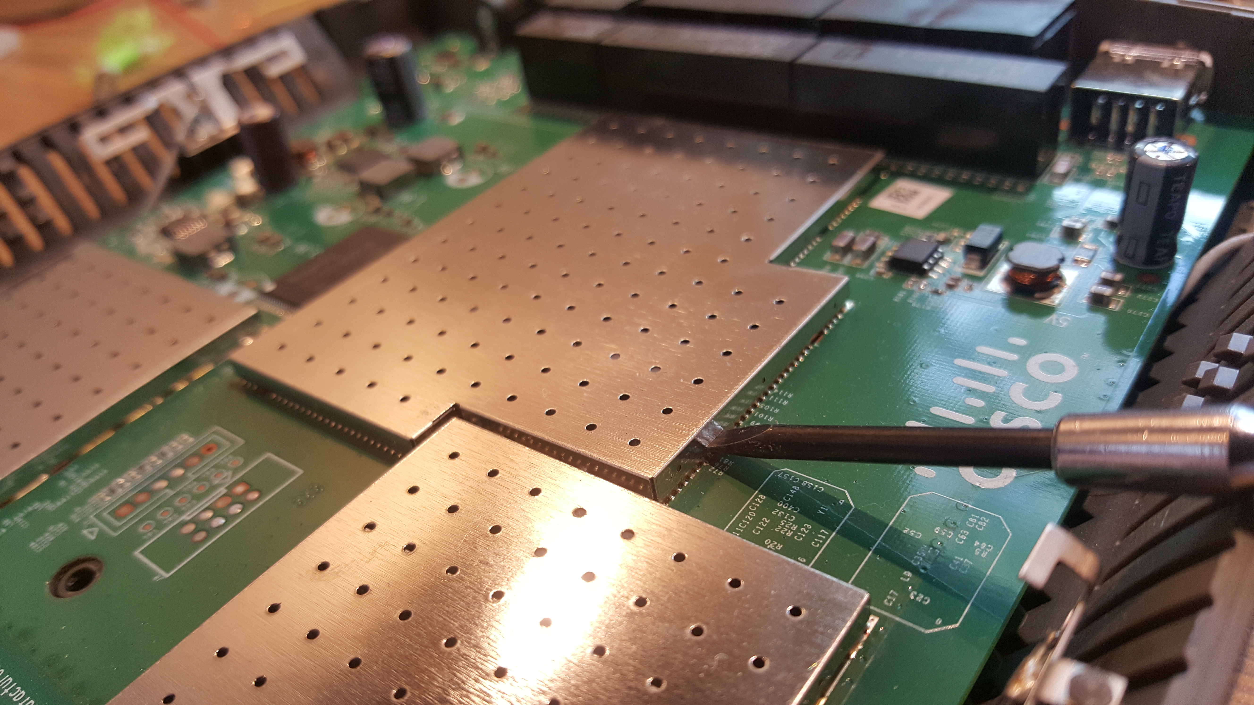
2. Remove the RF shield that covers the SoC
- Pry between the PCB and the outside of the RF shield with a small flat head screw driver. The top of the RF shield will come off once it’s loosened on all sides. This is a picture of the shield on the EA3500. It is very similar in the EA4x00 series.
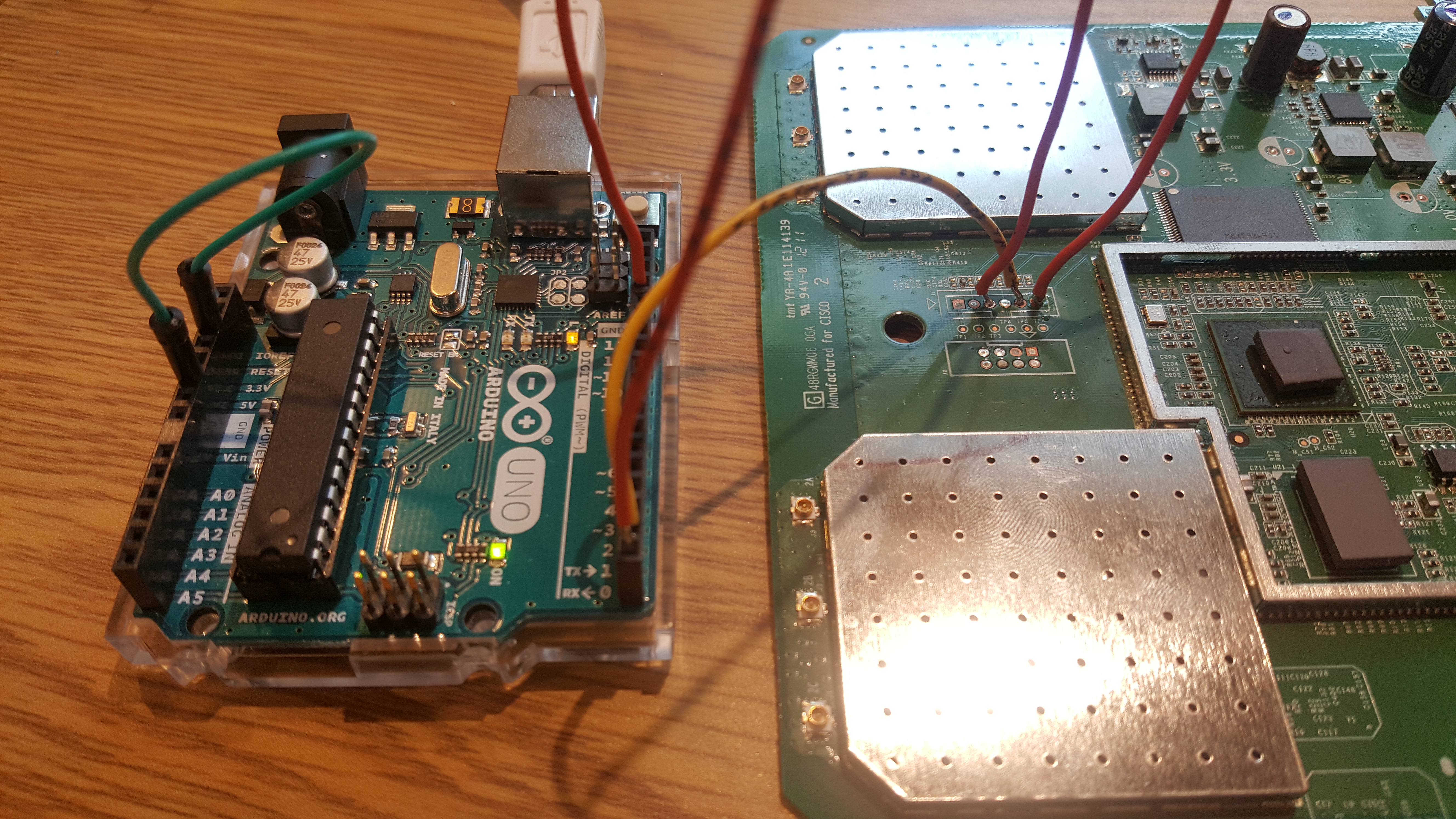
3. Connect to the router’s serial console
-
Solder on the Ground, RX, and TX connections on the serial port header. It’s helpful to use your multimeter to make sure you connect to the ground pin for the serial port. The pin-out is the same for both the EA3500 and EA4x00 series.
If you connect VCC to Ground or vice-versa you will risk damaging the router or your serial converter / port.
Pin Connection 1 VCC (don’t connect) 2 3 RX 4 5 TX 6 GND -
I’m using an Arduino Uno as a USB to Serial interface connected to the Linksys EA3500.
4. Start your Terminal
-
I use
minicomon my Linux machine as a terminal emulator to access the console the router.minicom /dev/ttyACM0 -b 115200 -
If you are successful, you should see the below text appear when you boot up the router.
-
Try swapping RX and TX if you don’t see any output.
-
EA3500
__ __ _ _ | \/ | __ _ _ ____ _____| | | | |\/| |/ _` | '__\ \ / / _ \ | | | | | | (_| | | \ V / __/ | | |_| |_|\__,_|_| \_/ \___|_|_| _ _ ____ _ | | | | | __ ) ___ ___ | |_ | | | |___| _ \ / _ \ / _ \| __| | |_| |___| |_) | (_) | (_) | |_ \___/ |____/ \___/ \___/ \__| ** WNC BOARD: audi R2.2 LE ** U-Boot 1.1.4 (Jan 2 2012 - 19:59:08) Marvell version: 3.5.9 U-Boot code: 00600000 -> 0067FFF0 BSS: -> 006CFB20 Soc: 88F6282 A1CPU running @ 800Mhz L2 running @ 400Mhz SysClock = 400Mhz , TClock = 200Mhz -
EA4x00
         __  __                      _ _
        |  \/  | __ _ _ ____   _____| | |
        | |\/| |/ _` | '__\ \ / / _ \ | |
        | |  | | (_| | |   \ V /  __/ | |
        |_|  |_|\__,_|_|    \_/ \___|_|_|
 _   _     ____              _
| | | |   | __ )  ___   ___ | |_
| | | |___|  _ \ / _ \ / _ \| __|
| |_| |___| |_) | (_) | (_) | |_
 \___/    |____/ \___/ \___/ \__|
 ** WNC BOARD: Viper R2.2 LE **
 ** For Development Only. Not For Demo **

U-Boot 1.1.4 (Sep 15 2011 - 15:46:36) Marvell version: 3.5.9

U-Boot code: 00600000 -> 0067FFF0  BSS: -> 006CFB20

Soc: 88F6282 A1CPU running @ 1200Mhz L2 running @ 400Mhz
SysClock = 400Mhz , TClock = 200Mhz
-
Now the steps differ for the EA3500 and EA4x00 Series. Click on the links below to take you to the steps for the router that you are overclocking.
Linksys EA3500
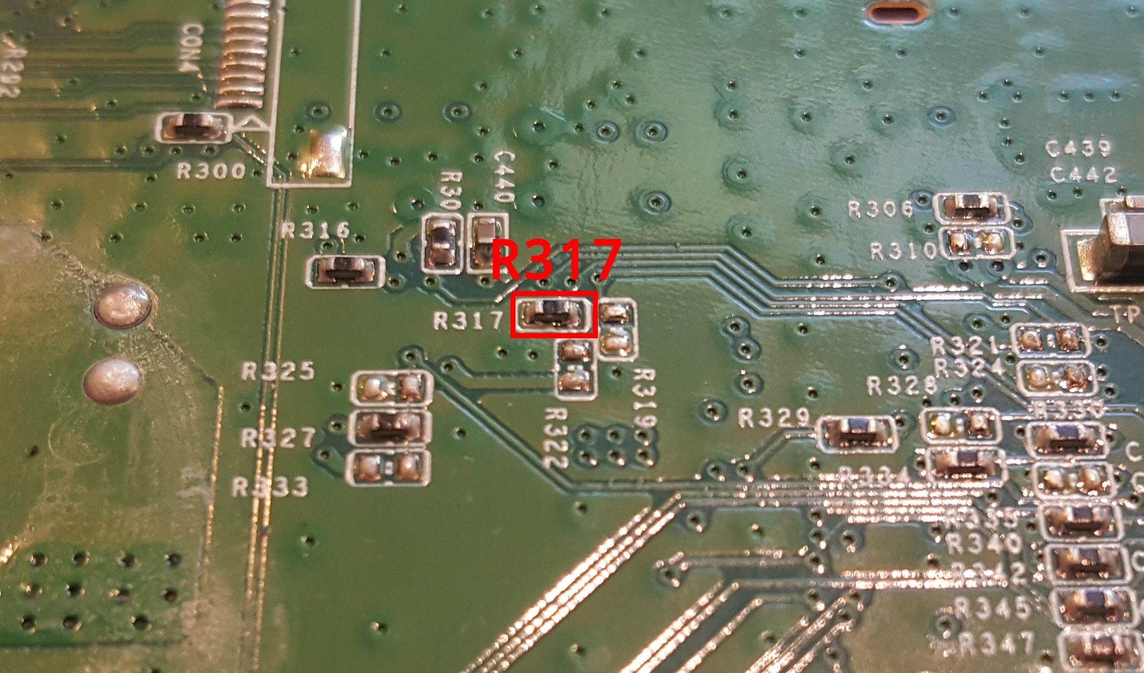
5. DDR Ratio - Remove R317
-
The Linksys EA3500 defaults at a DDR ratio of 2:1. We need to change the ratio to 4:1 so that the DDR clock will run at 450MHz when we change the CPU speed to 1800MHz.
-
All we need to do is remove R317 on the back of the board, because this bit is pulled down by default internally in the SoC. To remove the SMD resistor carefully use the small flathead screwdriver to very gently push the resistor while alternating heat on both pads of the resistor with your soldering iron. When the solder starts to flow, the resistor should start to move and it should slide off of the pads on the PCB. Do not push too hard on the resistor otherwise you might break the resistor or worse break off the PCB pad and you won’t be able to solder it back on.
-
After you remove the resistor, save it for later in case you damage or loose a resistor in future steps
-
Unplug your serial connection and the power before soldering. Most soldering irons are connected directly to line current and the current will flow to anything grounded including your serial adapter, and computer. Simply unplugging the serial port or the USB connection is good enough.
Remove R317 (on back of the board)
-
After you removed the resistor, connect up your serial adapter again and power up the router. If you are successful, you’ll see that the DDR frequency now reports 200MHz, which is a 4:1 ratio with the CPU clock speed.
         __  __                      _ _
        |  \/  | __ _ _ ____   _____| | |
        | |\/| |/ _` | '__\ \ / / _ \ | |
        | |  | | (_| | |   \ V /  __/ | |
        |_|  |_|\__,_|_|    \_/ \___|_|_|
 _   _     ____              _
| | | |   | __ )  ___   ___ | |_
| | | |___|  _ \ / _ \ / _ \| __|
| |_| |___| |_) | (_) | (_) | |_
 \___/    |____/ \___/ \___/ \__|
 ** WNC BOARD: audi R2.2 LE **

U-Boot 1.1.4 (Jan  2 2012 - 19:59:08) Marvell version: 3.  5.9

U-Boot code: 00600000 -> 0067FFF0  BSS: -> 006CFB20

Soc: 88F6282 A1CPU running @ 800Mhz L2 running @ 400Mhz
SysClock = 200Mhz , TClock = 200Mhz
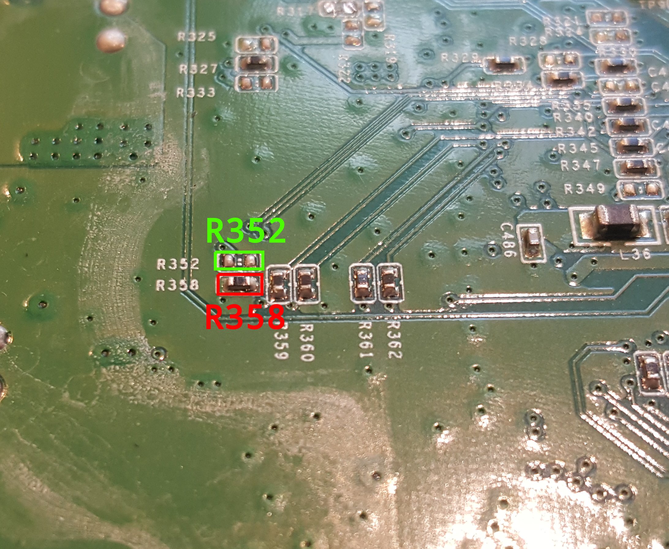
6. L2 Ratio - Move R358 to R352
-
The EA3500 defaults the L2 cache ratio to 2:1, and we need to change it to 4:1 so it runs at 450MHz when we overclock to 1800MHz.
-
For this we’ll need to move R358 (low) to R352 (high) which will change the most significant bit of the L2 clock configuration from 0 to 1.
Move R358 to R352 (on back of the board)
-
Connect your serial port and boot up again. You will see that the L2 Cache is now reporting to be 200MHz.
         __  __                      _ _
        |  \/  | __ _ _ ____   _____| | |
        | |\/| |/ _` | '__\ \ / / _ \ | |
        | |  | | (_| | |   \ V /  __/ | |
        |_|  |_|\__,_|_|    \_/ \___|_|_|
 _   _     ____              _
| | | |   | __ )  ___   ___ | |_
| | | |___|  _ \ / _ \ / _ \| __|
| |_| |___| |_) | (_) | (_) | |_
 \___/    |____/ \___/ \___/ \__|
 ** WNC BOARD: audi R2.2 LE **

U-Boot 1.1.4 (Jan  2 2012 - 19:59:08) Marvell version: 3.5.9

U-Boot code: 00600000 -> 0067FFF0  BSS: -> 006CFB20

Soc: 88F6282 A1CPU running @ 800Mhz L2 running @ 200Mhz
SysClock = 200Mhz , TClock = 200Mhz
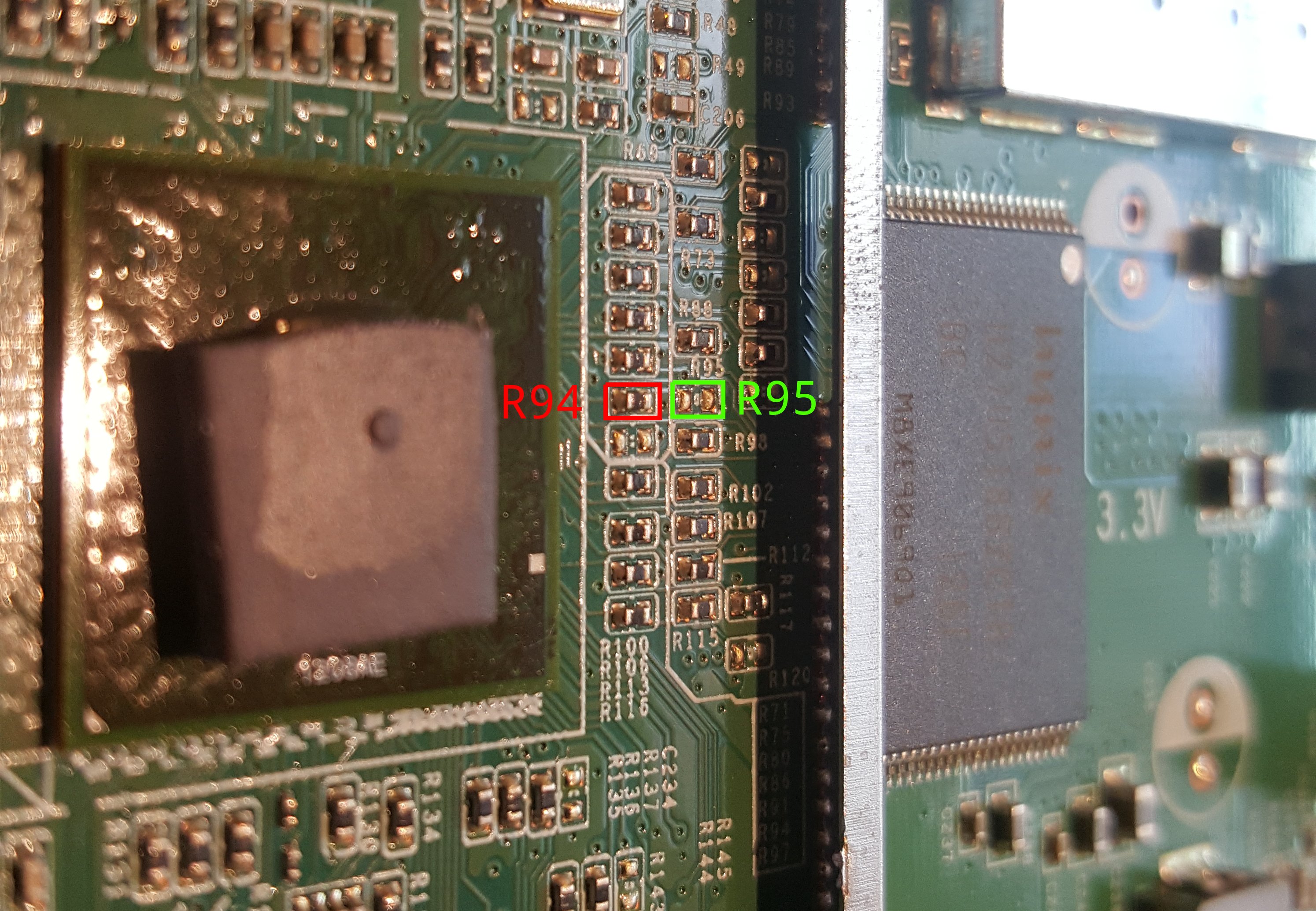
7. CPU Clock - Move R94 to R95
-
Now here’s where we finally overclock the device. The EA3500’s default CPU configuration is 800MHz which is represented as
0110. All we need to do is flip the most significant bit to achieve1110and 1800MHz. -
On the center left of the SoC is resistor R94. Move it to R95.
Move R94 to R95 (center left of Soc)
-
When you’re successful you will see that the CPU clock reports as 1800MHz and the DDR and L2 Cache report as 450MHz
         __  __                      _ _
        |  \/  | __ _ _ ____   _____| | |
        | |\/| |/ _` | '__\ \ / / _ \ | |
        | |  | | (_| | |   \ V /  __/ | |
        |_|  |_|\__,_|_|    \_/ \___|_|_|
 _   _     ____              _
| | | |   | __ )  ___   ___ | |_
| | | |___|  _ \ / _ \ / _ \| __|
| |_| |___| |_) | (_) | (_) | |_
 \___/    |____/ \___/ \___/ \__|
 ** WNC BOARD: audi R2.2 LE **

U-Boot 1.1.4 (Jan  2 2012 - 19:59:08) Marvell version: 3.5.9

U-Boot code: 00600000 -> 0067FFF0  BSS: -> 006CFB20

Soc: 88F6282 A1CPU running @ 1800Mhz L2 running @ 450Mhz
SysClock = 450Mhz , TClock = 200Mhz
8. Install the Heatsink
-
Now all you have left to do is install the heatsink.
-
I just applied heatsink compound to the top of the RF shield and super-glued a scrap heatsink that I had lying around. This seems to be adequate for stable operation in room temperature.
Congratulations!
You’ve successfully overclocked your Linksys EA3500 router!
If you haven’t already, you should flash OpenWrt to it. https://openwrt.org/toh/linksys/ea3500#installation
Linksys EA4x00
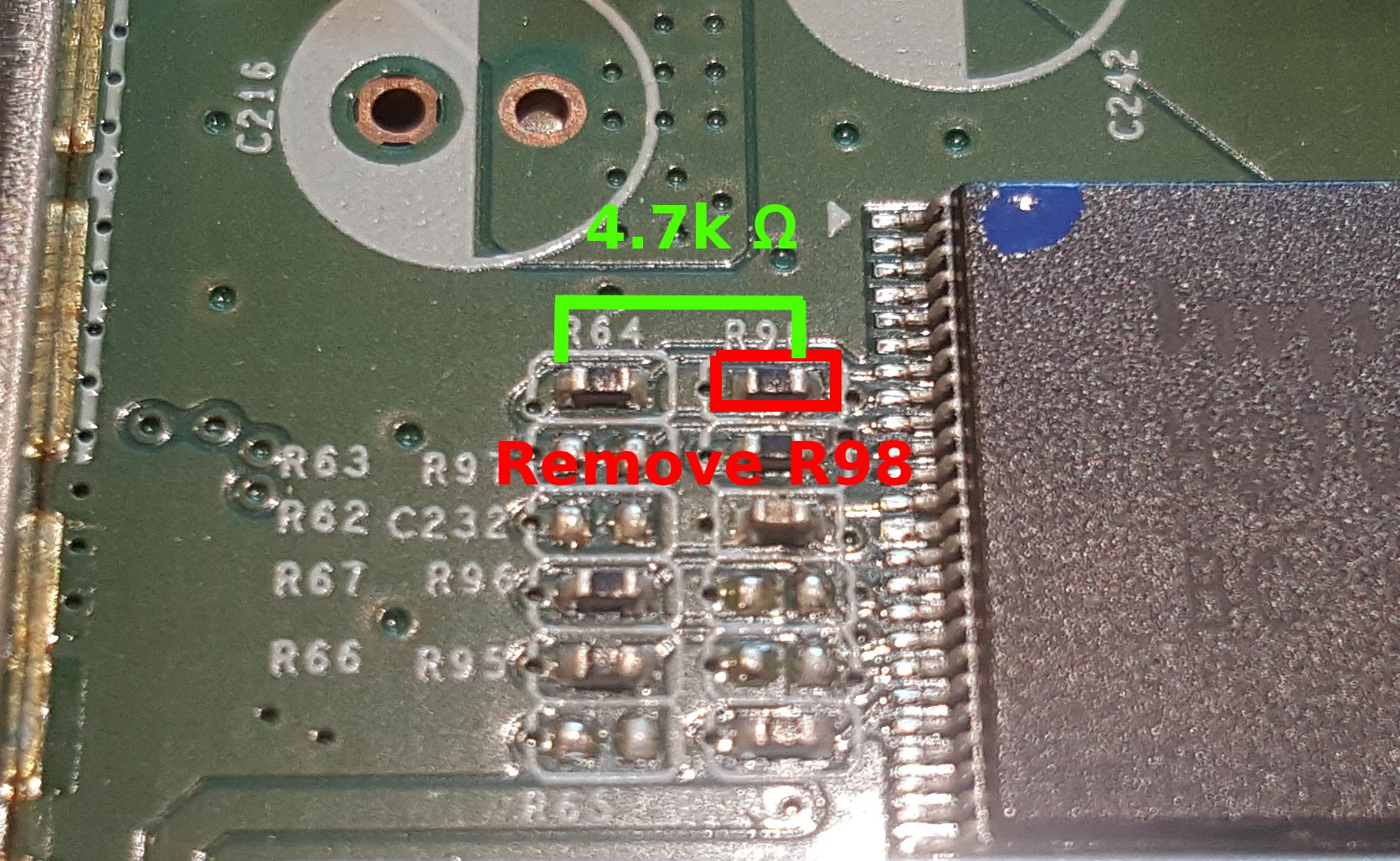
5. DDR Ratio - Remove R98 and pull R98 high
-
The Linksys EA4x00 defaults at a DDR ratio of 3:1. We need to change the ratio to 4:1 so that the DDR clock will run at 500MHz when we change the CPU speed to 2000MHz.
-
We need to remove R98 and then put a 4.7k ohm resistor in it’s place connected to VCC so we can pull this bit high. To remove the SMD resistor carefully use the small flathead screwdriver to very gently push the resistor while alternating heat on both pads of the resistor with your soldering iron. When the solder starts to flow, the resistor should start to move and it should slide off of the pads on the PCB. Do not push too hard on the resistor otherwise you might break the resistor or worse break off the PCB pad and you won’t be able to solder it back on.
-
After you remove the resistor, save it for later in case you damage or loose a resistor in future steps
-
Unplug your serial connection and the power before soldering. Most soldering irons are connected directly to line current and the current will flow to anything grounded including your serial adapter, and computer. Simply unplugging the serial port or the USB connection is good enough.
Remove R98 and connect 4.7k resistor to VCC (next to NAND)
Before
After
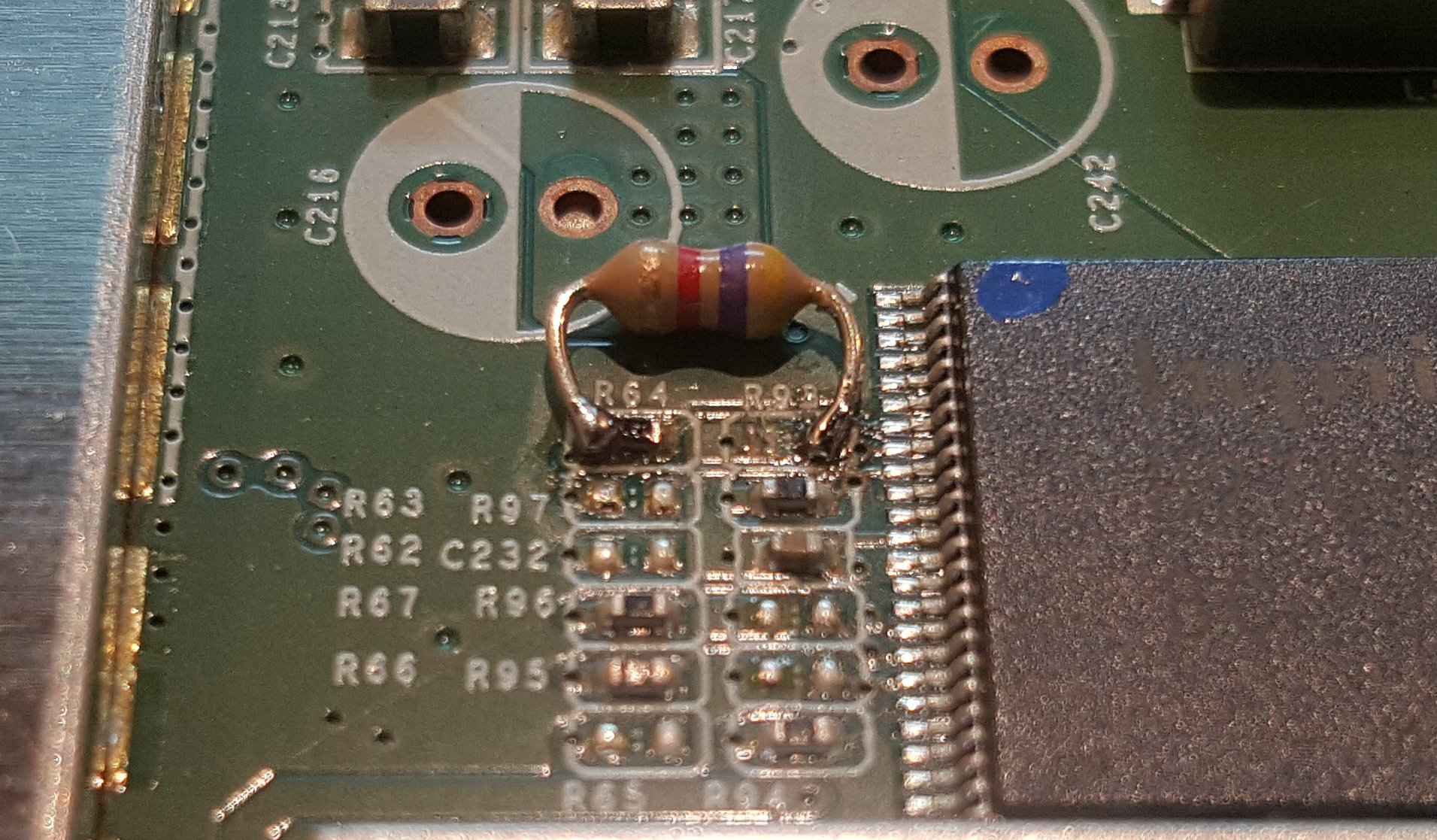 I used a small 4.7k Ohm resistor and connected the R98 pad to the VCC on R64
 -
After you’re done, connect up your serial adapter again and power up the router. If you are successful, you’ll see that the DDR frequency now reports 300MHz, which is a 4:1 ratio with the CPU clock speed.
         __  __                      _ _
        |  \/  | __ _ _ ____   _____| | |
        | |\/| |/ _` | '__\ \ / / _ \ | |
        | |  | | (_| | |   \ V /  __/ | |
        |_|  |_|\__,_|_|    \_/ \___|_|_|
 _   _     ____              _
| | | |   | __ )  ___   ___ | |_
| | | |___|  _ \ / _ \ / _ \| __|
| |_| |___| |_) | (_) | (_) | |_
 \___/    |____/ \___/ \___/ \__|
 ** WNC BOARD: Viper R2.2 LE **
 ** For Development Only. Not For Demo **

U-Boot 1.1.4 (Sep 15 2011 - 15:46:36) Marvell version: 3.5.9

U-Boot code: 00600000 -> 0067FFF0  BSS: -> 006CFB20

Soc: 88F6282 A1CPU running @ 1200Mhz L2 running @ 400Mhz
SysClock = 300Mhz , TClock = 200Mhz
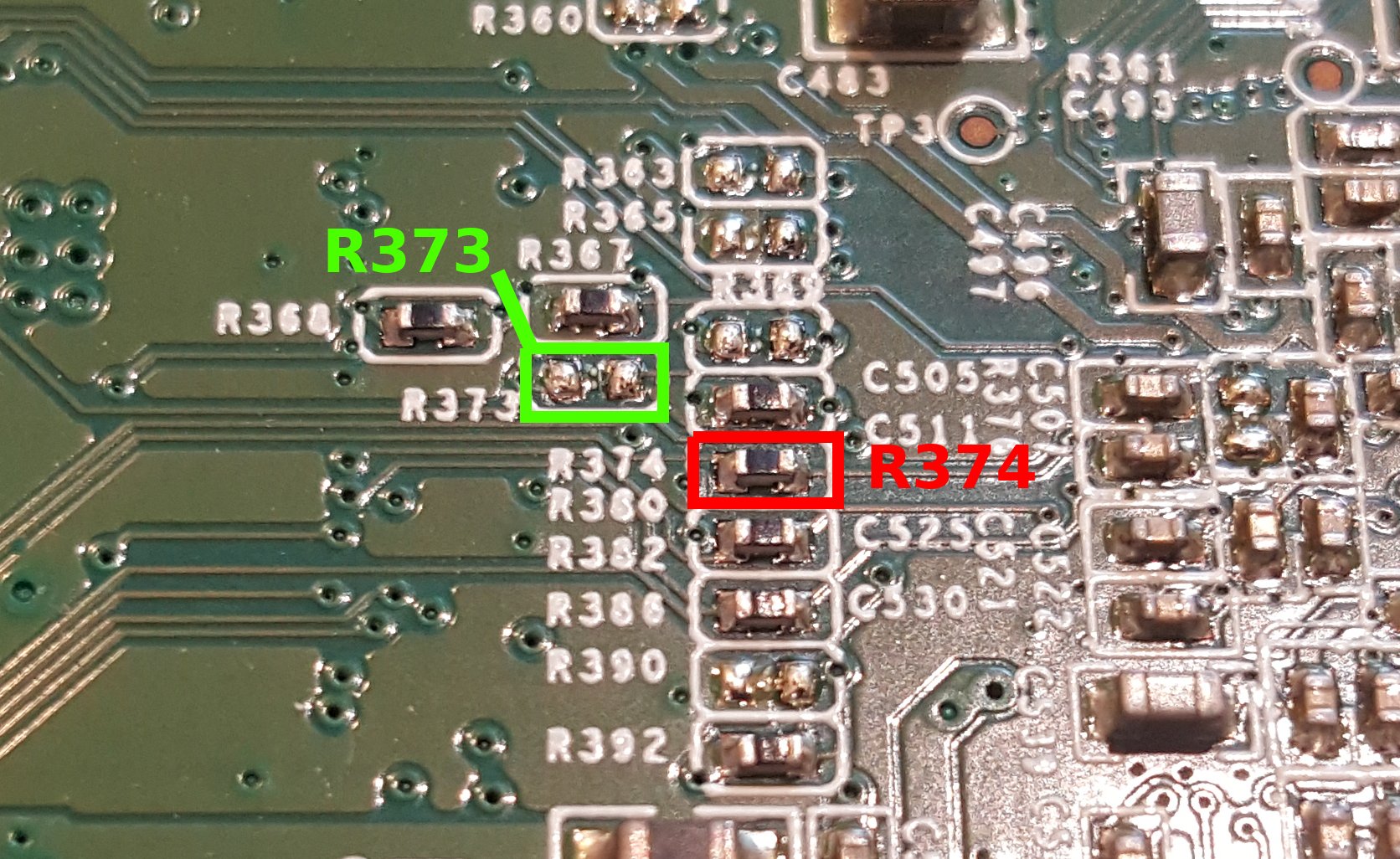
6. CPU Clock - Move R374 to R373
-
Next we’re going to move the CPU clock speed up to 1600MHz by moving the second most significant bit of the CPU clock configuration. On the back of the board, remove R374 and solder it onto R373 to pull this bit high. Don’t forget to unplug your serial adapter before soldering.
Move R374 to R373 (back of the board)
-
When you’re done, connect up your serial port and power on the router. You’ll see that the CPU clock speed has changed to 1600MHz and the DDR and L2 speeds have also increased.
         __  __                      _ _
        |  \/  | __ _ _ ____   _____| | |
        | |\/| |/ _` | '__\ \ / / _ \ | |
        | |  | | (_| | |   \ V /  __/ | |
        |_|  |_|\__,_|_|    \_/ \___|_|_|
 _   _     ____              _
| | | |   | __ )  ___   ___ | |_
| | | |___|  _ \ / _ \ / _ \| __|
| |_| |___| |_) | (_) | (_) | |_
 \___/    |____/ \___/ \___/ \__|
 ** WNC BOARD: Viper R2.2 LE **
 ** For Development Only. Not For Demo **

U-Boot 1.1.4 (Sep 15 2011 - 15:46:36) Marvell version: 3.5.9

U-Boot code: 00600000 -> 0067FFF0  BSS: -> 006CFB20

Soc: 88F6282 A1CPU running @ 1600Mhz L2 running @ 533Mhz
SysClock = 400Mhz , TClock = 200Mhz
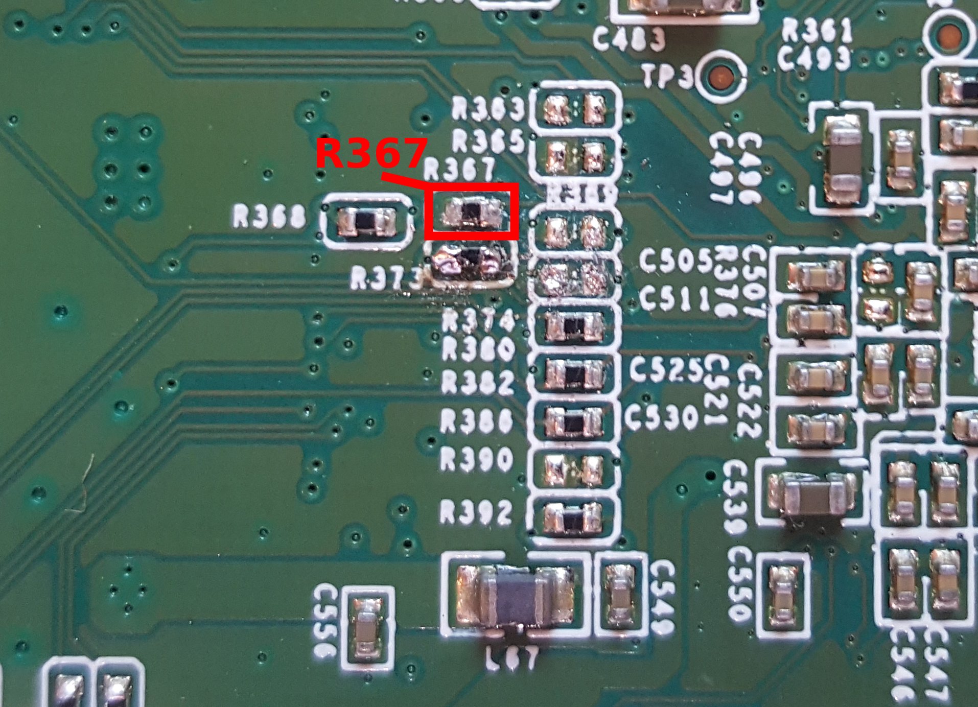
7. CPU Clock - Remove R367
-
Finally we’re going to move the CPU clock speed up to 2000MHz by moving the third most significant bit of the CPU clock configuration. On the back of the board, all we need to do is remove R367 to set this bit high because the SoC defaults this as pull up. Don’t forget to unplug your serial port before soldering
Remove R367
-
When you’re done, connect up your serial port and power on the router. You’ll see that the CPU clock speed has changed to 2000MHz and the DDR and L2 speeds have also increased.
         __  __                      _ _
        |  \/  | __ _ _ ____   _____| | |
        | |\/| |/ _` | '__\ \ / / _ \ | |
        | |  | | (_| | |   \ V /  __/ | |
        |_|  |_|\__,_|_|    \_/ \___|_|_|
 _   _     ____              _
| | | |   | __ )  ___   ___ | |_
| | | |___|  _ \ / _ \ / _ \| __|
| |_| |___| |_) | (_) | (_) | |_
 \___/    |____/ \___/ \___/ \__|
 ** WNC BOARD: Viper R2.2 LE **
 ** For Development Only. Not For Demo **

U-Boot 1.1.4 (Sep 15 2011 - 15:46:36) Marvell version: 3.5.9

U-Boot code: 00600000 -> 0067FFF0  BSS: -> 006CFB20

Soc: 88F6282 A1CPU running @ 2000Mhz L2 running @ 666Mhz
SysClock = 500Mhz , TClock = 200Mhz
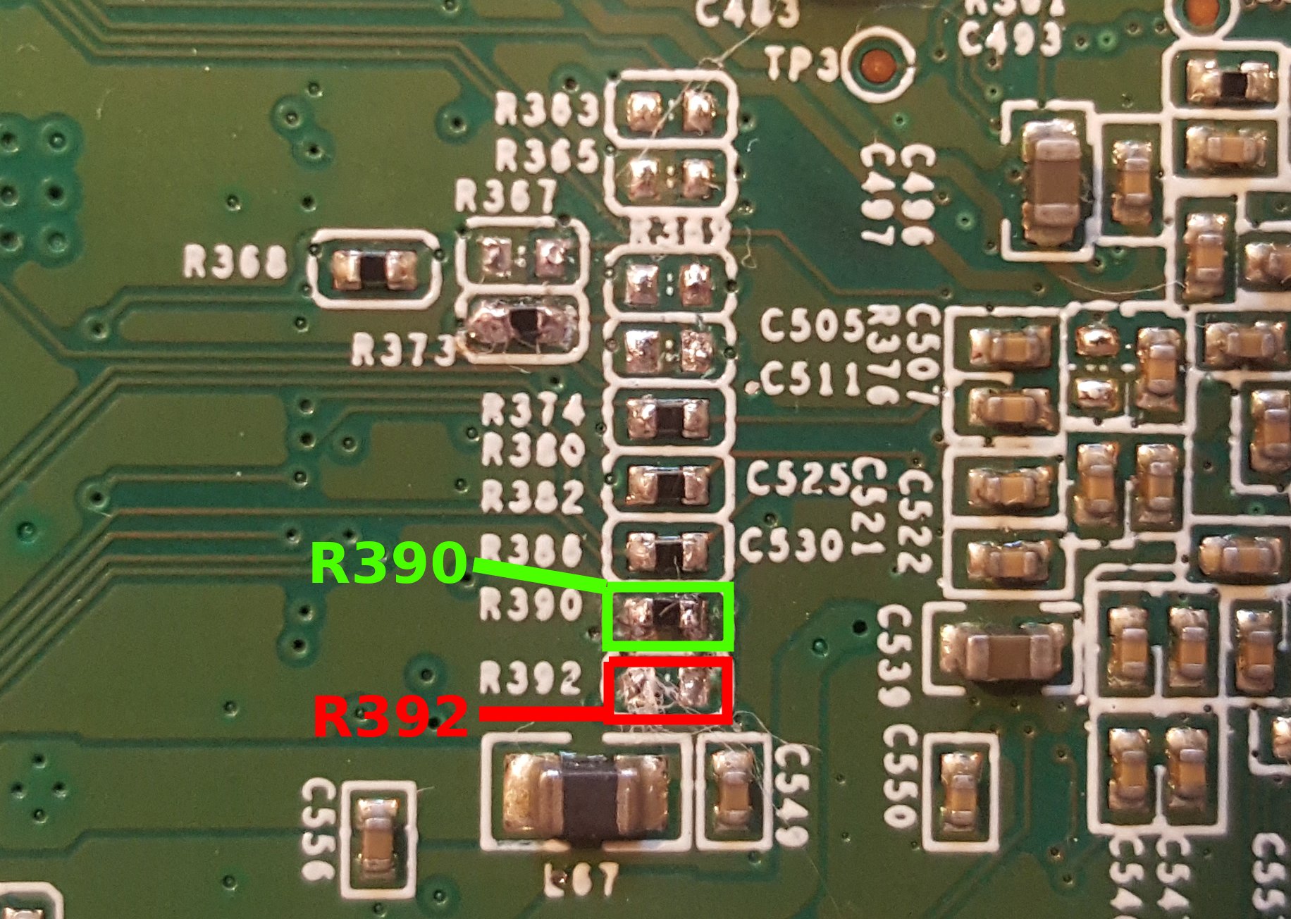
If you have instability…
-
Until now, I’ve been referring to the Linksys EA4200 and EA4500 as the EA4x00 series because they share an identical PCB layout; however, there is a small difference between the two. I was unable to overclock the EA4200 to 2000MHz like I was the EA4500. I believe this is because the two models use different DDR ram chips, and the EA4500 supports a higher clock speed at 500MHz, but I haven’t confirmed this is the reason. If you experience instability with your EA4x00 device, you can down clock to 1800MHz.
-
Also, if you don’t want to add a fan to your router, you can perform this step so that a passive heatsink will be enough for heat dissipation.
-
To down clock from 2000MHz to 1800MHz, move R392 to R390 to pull the least significant bit low for the CPU clock configuration.
Move R392 to R390
-
After you’re done, connect your serial port and boot up the device. You’ll see that the CPU clock is at 1800MHz and the DDR and L2 clocks have decreased.
         __  __                      _ _
        |  \/  | __ _ _ ____   _____| | |
        | |\/| |/ _` | '__\ \ / / _ \ | |
        | |  | | (_| | |   \ V /  __/ | |
        |_|  |_|\__,_|_|    \_/ \___|_|_|
 _   _     ____              _
| | | |   | __ )  ___   ___ | |_
| | | |___|  _ \ / _ \ / _ \| __|
| |_| |___| |_) | (_) | (_) | |_
 \___/    |____/ \___/ \___/ \__|
 ** WNC BOARD: Viper R2.2 LE **
 ** For Development Only. Not For Demo **

U-Boot 1.1.4 (Sep 15 2011 - 15:46:36) Marvell version: 3.5.9

U-Boot code: 00600000 -> 0067FFF0  BSS: -> 006CFB20

Soc: 88F6282 A1CPU running @ 1800Mhz L2 running @ 600Mhz
SysClock = 450Mhz , TClock = 200Mhz
8. Install the Heatsink and Fan
-
Now all you have left to do is install the heatsink.
-
If you clocked your device to 2000MHz, a small fan is recommended. I use an old graphics card heatsink and connected the power to 3.3V. It is very quiet and doesn’t move much air, but it makes a huge difference in how hot the device gets.
-
For this picture, I just applied heatsink compound to the top of the RF shield and super-glued a scrap heatsink that I had lying around. This seems to be adequate for stable operation in room temperature.
Congratulations!
You’ve successfully overclocked your Linksys EA4x00 router!
If you haven’t already, you should flash OpenWrt to it. https://openwrt.org/toh/linksys/ea4500#installation
Clock Configuration Tables
The Marvell Feroceon only supports certain combinations of CPU, DDR, and L2 speeds. The general recommendation is for the DDR speed to not exceed 400MHz and L2 speed to not exceed 500MHz. Also, it is recommended to have the L2 speed greater than the DDR speed.
You can read more about this in the Marvell 88R6281 datasheet.
When pulled low, a 4.7k ohm resistor is connected between the pin and ground. When pulled high, a 4.7k ohm resistor is connected between the pin and VCC (3.3V).
CPU Clock Speed
Pins:
- MPP[2] - NAND IO4
- MPP[5] - NAND IO7
- MPP[19] - NAND IO1
- MPP[10] - NAND R06
| CPU Speed | MPP[2] | MPP[5] | MPP[19] | MPP[10] | Notes |
|---|---|---|---|---|---|
| 800MHz | 0 | 1 | 1 | 0 | SoC Default, (default for EA3500) |
| 1000MHz | 0 | 1 | 1 | 1 | |
| 1200MHz | 1 | 0 | 0 | 1 | (default for EA4x00) |
| 1600MHz | 1 | 1 | 0 | 1 | |
| 1800MHz | 1 | 1 | 1 | 0 | (target for EA3500) (target for EA4200) |
| 2000MHz | 1 | 1 | 1 | 1 | (target for EA4500) |
DDR Ratios
Pins:
- MPP[33] - TX_CTL
- (I couldn’t find this pin. It is probably related to the network switch chip 88E6171R. I have the datasheet for the pin compatible equivalent 88E6350R, if you want to try to locate it. If you find it, please open a PR. I think it might allow the EA3500 to be clocked to 2.0GHz)
- NF_ALE - NAND ALE
- NF_REn - NAND RE
- NF_CLE - NAND CLE
| CPU to DDR | MPP[33] | NF_ALE | NF_REn | NF_CLE | Notes |
|---|---|---|---|---|---|
| 2:1 | 0 | 0 | 1 | 0 | (default for EA3500) |
| 2.5:1 | 0 | 0 | 1 | 1 | |
| 3:1 | 0 | 1 | 0 | 0 | SoC Default, (default for EA4x00) |
| 4:1 | 0 | 1 | 1 | 0 | (target for EA3500, EA4x00) |
| 4.5:1 | 0 | 1 | 1 | 1 | |
| 5:1 | 1 | 0 | 0 | 0 | (unable to find pin, but might allow 2.0GHz on EA3500) |
| 6:1 | 1 | 0 | 0 | 1 |
L2 Cache Ratios
- MPP[3] - NAND IO5
- MPP[12] - SD_CLK (I couldn’t find this pin but we don’t need to change it)
- NF_WEn - NAND Write Enable
| CPU to L2 | MPP[3] | MPP[12] | NF_WEn | Notes |
|---|---|---|---|---|
| 2:1 | 0 | 0 | 1 | SoC Default (internally pulled), (default for EA3500) |
| 2.5:1 | 0 | 0 | 1 | |
| 3:1 | 0 | 1 | 1 | (default / target for EA4x00) |
| 4:1 | 1 | 0 | 0 | (target for EA3500) |
| 4.5:1 | 1 | 0 | 1 |
Links
Here’s some further reading on overclocking the Feroceon.
Original inspiration for this project except for the 88F6281 (in Polish)